Shining a light on the nanoscale
15 Dec 2021
 |
Researchers in the US have managed to reveal nanoscale optical and electronic band information of 2D semiconducting materials, using visible light. By employing a hyper-focusing technique they developed previously, the team managed to push beyond the diffraction limits of visible light to achieve a resolution of just a few nanometres. They say that this technique could help characterize the nanoscale properties of 2D and 3D materials to improve our understanding of catalysis, quantum optics and nanoelectronics.
Advanced 2D and 3D materials, such as single-walled carbon nanotubes, hold a lot of promise for next-generation electronics. In use, the electronic and optical properties of these materials are influenced by their environment, such as localized defects, strains, dielectric screening and quantum effects that can alter their performance. Characterizing the nanoscale details that cause these issues can be challenging. But as the colour and optical properties of these nanomaterials are closely related to their electronic structures, a technique known as hyperspectral imaging could offer a solution.
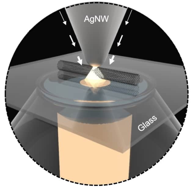
Hyperspectral imaging analyses the spectrum of every pixel in a scene across many wavelength bands. This electromagnetic detail can be used to obtain all sorts of information. For nanoscale materials, there has been some success using such techniques with wavelengths of light outside the visible range. Extending these techniques to the visible spectrum could allow more direct probing and simplify techniques, by eliminating the need for advanced light sources. With wavelengths of a few hundred nanometres, however, using visible light to obtain information from characteristics that are just a few nanometres in size is difficult. Ramping the resolution: White light from a tungsten lamp is focused into the tip of a silver nanowire. (Courtesy: CC BY 4.0/Nat. Commun. 10.1038/s41467-021-27216-5)
 Ramping the resolution: White light from a tungsten lamp is focused into the tip of a silver nanowire. (Courtesy: CC BY 4.0/Nat. Commun. 10.1038/s41467-021-27216-5)
To tackle this problem, Ming Liu, a physicist at the University of California, Riverside, and his colleagues have developed a technique known as super-focusing. The method integrates a tapered glass optical fibre with a silver nanowire condenser. “We can couple almost all the light from an optical fibre into a silver nanowire,” Liu tells Physics World.
Liu explains that as the light travels along the tapered optical fibre its wavelength gradually increases. As it reaches the end of the optical fibre, the wavelength matches that of the electron density wave in the silver nanowire.
Free electrons on the silver nanowire are then driven by the energy of the light and start to oscillate. These electrons then carry the energy along the surface of the silver nanowire. According to Liu, you can imagine this as being like a wave on the ocean being driven by the energy of the wind. At the end of the nanowire, a spot of light is produced – “like waves coming into a bay and its tapered shape producing a tsunami,” Liu adds.
All this means that the possible resolution is no longer limited by the wavelength of light. “We use the electron wave to carry the electromagnetic wave, instead of the light photons,” Liu explains. “Now the ultimate wavelength is restricted by the wavelength of electrons, which is very, very short: nanometre scale.”
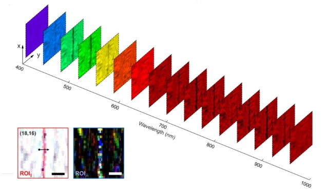
In their latest work, described in Nature Communications, the researchers demonstrated that using this super-focusing technique they can achieve a 6 nm spatial resolution using visible to near-infrared wavelengths (415–980 nm) while probing single-walled carbon nanotubes. This allowed them to characterize nanoscale details such as chirality and electrical band structure.
“We showed the colour, but actually the colour is kind of determined by the electrical properties of the material,” Liu explains. “So, what we really want to say is that it can see the electrical band structures.” That is the transitions between the different band structures: how large those band gaps are.
Being able to characterize such nanoscale details – as opposed to the global performance – of 2D and 3D materials will help with the development of advanced semiconductors and newer techniques like twistronics, Liu says. He and his colleagues are now trying to see whether they can push the resolution as low as 1 nm.
Michael Allen is a science writer based in the UK
from physicsworld.com 17/12/2021
Δεν υπάρχουν σχόλια:
Δημοσίευση σχολίου