Champion semiconductor could replace silicon, say researchers
01 Aug 2022
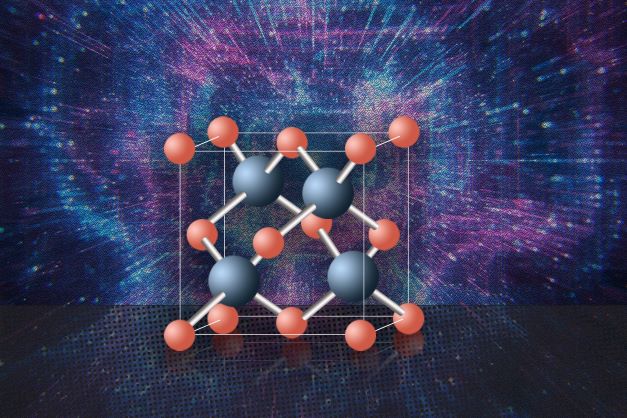
Power cube: Researchers claim that cubic boron arsenide is the best semiconducting material ever found, and perhaps even the best possible one. (Courtesy: Christine Daniloff/MIT)
Cubic boron arsenide is one of the best semiconductors known to science and could even dethrone silicon as the principal component of modern electronics. This finding, from teams headed by Gang Chen at the Massachusetts Institute of Technology in the US and Xinfeng Liu of the National Center for Nanoscience and Technology in Beijing, China, is based on experiments showing that small, pure regions of the material display a thermal conductivity and charge carrier mobility that far outperforms those of existing widely-used semiconductors, including silicon. The results validate theoretical predictions and suggest that cubic boron arsenide could revolutionize the field of electronics – at least in principle.
Silicon has dominated the electronics industry for decades. It is relatively easy to purify into a material with an almost perfectly uniform molecular lattice – an important requirement for robust and reliable electronic properties – and its status as one of the most abundant elements in Earth’s crust makes it commercially viable to use at scale.
Silicon’s performance as a semiconductor, however, leaves much to be desired. The issues with the material are twofold. The first concerns the mobility of its “holes”, which are regions of positive charge left behind when electrons are excited from a semiconductor’s insulating (valence) band to its conduction band. In silicon, these holes move much more slowly than the electrons in the conduction band, diminishing the material’s electrical performance. The second issue is silicon’s low thermal conductivity, which makes silicon-based electronic systems prone to overheating: a problem that can only be mitigated with costly cooling systems.
Reduced defects yield desirable properties
Several recent theoretical studies have predicted far more desirable properties in cubic boron arsenide (c-BA). According to these calculations, the material’s thermal conductivity should be some 10 times higher than silicon’s, stemming from its unique chemical bonding properties. Theorists also predicted simultaneously high mobilities of electrons and holes at room temperature. Hard to synthesize: Single crystals of boron arsenide. (Courtesy: University of Houston)
 Hard to synthesize: Single crystals of boron arsenide. (Courtesy: University of Houston)
Until now, however, these promising predictions haven’t been borne out in experiments. The problem is that with existing fabrication methods, c-BA crystals typically feature large, non-uniform concentrations of defects, leading to significant discrepancies with predicted behaviour.
In the latest studies, which are described in back-to-back papers in Science, members of the two teams used a combination of spectroscopic techniques to precisely map out the distribution of impurities within thin c-BA samples. This allowed them to identify local regions of uniformity in its molecular lattice, free from impurities. Within these regions, the material’s semiconducting properties were some of the best ever measured, displaying exceptional values for thermal conductivity and hole mobility that were similar to those predicted from first-principles calculations.READ MORE

Despite this promising discovery, it remains to be seen whether c-BA has a realistic chance of replacing silicon. Both boron and arsenic are far less abundant than silicon in the Earth’s crust, and researchers would need to substantially improve the purity of the material during fabrication for large-scale applications to be feasible. However, if these barriers can be overcome, Zhifeng Ren, director of the Texas Center for Superconductivity at the University of Houston, US and a corresponding author on both studies, says the discovery could have an impact similar to the advances in electronics that followed the advent of silicon wafers.
Sam Jarman is a science writer based in the UK.
from physicswold.com 10/8/2022

Δεν υπάρχουν σχόλια:
Δημοσίευση σχολίου