Graphene twists again
22 Oct 2018 Belle Dumé

Umklapp electron-electron scattering in so-called moiré superlattices made from aligned layers of 2D materials such as graphene and hexagonal boron nitride could degrade the high-temperature mobility of graphene’s charge carriers. This is the new result from researchers in the UK, US and Japan who say the effect would limit the potential applications of these technologically important materials in room-temperature high-mobility devices. The problem could be overcome, however, by misaligning, or twisting, the 2D layers with respect to each other.
Umklapp electron-electron (Uee) scattering is the only intrinsic mechanism that allows electrons to transfer momentum to the crystal lattice and this gives pure metals an electrical resistance, explain the researchers led by Vladimir Fal’ko and Andre Geim of the National Graphene Institute at the University of Manchester in the UK. Uee is difficult to measure in an experiment, however, since it is often masked by other dissipation phenomena.
Uee processes lead to giant excess resistivity
Fal’ko and colleagues have now shown that Uee scattering dominates the transport properties of superlattices made from graphene layers placed on top of hexagonal boron nitride (hBN). The Uee processes at play in these heterostructures lead to giant excess resistivity that rapidly increases as the superlattice period increases and deteriorates their room temperature mobility by more than an order of magnitude when compared to ordinary, non-superlattice graphene devices.READ MORE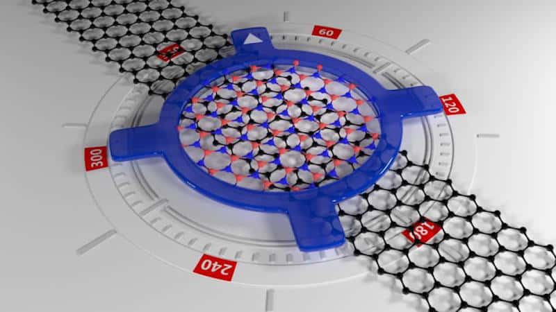
The researchers engineered their superlattices by aligning graphene with an hBN substrate. This process produces a moiré pattern because of the small lattice mismatch (of 1.8%) between the two materials. The moiré lattice formed has a periodic potential, λ, of around 15 nm when the two materials are perfectly aligned. This potential acts on charge carriers (electrons and holes) in graphene, dramatically altering the material’s electronic spectrum, making it go from being a “zero-gap” semiconductor without a band gap to one that does have a band gap.
Mini Brillouin zone forms around the Dirac point
A zero-gap semiconductor is one in which the electron valence and conduction bands just touch each other (at the so-called Dirac point). This is completely different to what happens in conventional semiconductors, which have an energy gap between the bands. At the Dirac point, the relationship between the energy and momentum of the electrons can be described by the Dirac equation and resembles that of a photon, with the electrons moving at a very high, relativistic, speed.

One of the most important things to happen in a moiré superlattice is the creation of a mini Brillouin zone around the Dirac point. The size of this zone depends on the misalignment angle, θ, between the graphene and hBN and the resulting moiré period λ. Since the Brillouin zone is small compared to that in normal metals, Uee scattering is the dominant effect in graphene/hBN superlattices, say the researchers, who obtained their result by measuring the resistivity of different superlattice devices and a “reference” device in which the graphene and hBN were intentionally misaligned by more than 15°. This device had a λ of less than 3 nm.
Twisting could solve the problem
“Uee scattering in long period moiré superlattice degrades the intrinsic high-temperature mobility of graphene’s charge carriers,” they report in Nature Physics 10.1038/s41567-018-0278-6. “This limits the potential applications of epitaxially-grown graphene/hBN heterostructures, which are inherently aligned, for room-temperature high-mobility devices.”
The 2D crystals that form the heterostructure should thus be misaligned, or twisted, if we are to achieve high carrier mobility at room temperature, they advise.

22/10/2018 from physicsworld.com
Δεν υπάρχουν σχόλια:
Δημοσίευση σχολίου