Dielectric nano bowties allow ultrahigh light confinement
14 Sep 2018 Michela Picardi
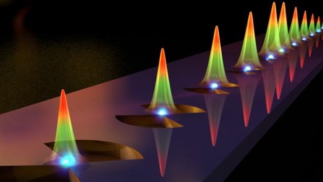
 Artistic rendering of the bowtie PhC. Credit: Ella Maru Studio
Matching the subwavelength confinement capabilities of plasmonic resonators, with the ultralow losses and cavity lifetimes of photonic crystals may be a step closer thanks to the work of a team lead by Sharon Weiss from the Electrical Engineering and Computer Science Department of Vanderbilt University (US). The researchers have, for the first time, experimentally demonstrated light confinement in a silicon “bowtie” crystal cavity. Published in Science, the article confirms the theoretical prediction that the group made in 2016 and paves the way towards all-dielectric field enhancement and confinement, crucial for applications in photovoltaic, computing, sensing, and quantum optics.
Confining light in a subwavelength volume is a longstanding challenge. It is attractive as it circumvents the traditional diffraction limit of optical microscopes, allowing smaller areas to be probed. Moreover, the associated local field enhancement induces a strong light-matter interaction, which could be manipulated to produce next-generation photonic technologies.
One way of trapping light is through temporal confinement, in which the light is kept inside a cavity of quality factor, Q for as long as possible. Indeed, dielectric-based cavities can have very high Q-factors making them well-equipped to retain incident light. But in contrast to their plasmonic counterparts, the confinement of light in a dielectric nanostructure is diffraction-limited, meaning that the volume of light that the cavity holds can never be substantially smaller than the incident wavelength.
In contrast to conventional photonic crystals, however, the lattice holes of this cavity present a dielectric inclusion in the shape of a nano bowtie, which further acts to localize light between its tips. This two-step phenomenon is effective in preserving the high Q factors of the photonic crystal cavity while achieving a strong spatial confinement of the light on the tips of the bowtie.In this recent work, Weiss and colleagues have managed to combine high Q factors with modal volumes comparable to those achieved by plasmonic structures, using a photonic crystal cavity whose unit cells are bowtie shaped. This strong confinement is underpinned by what they call a “two-steps localization process”. The first confinement step is that of any photonic material, due to the contrast in refractive index between the two constituent materials of the crystal, in this case silicon with air holes. The different refractive indexes of the structure force light to be scattered in certain preferential directions and prevent it from propagating in others. This is fully analogous to the way the atomic potential creates bandgaps for the electrons of a crystal and has therefore been called the photonic bandgap effect.
The experiment
To fabricate such an effective material, precise nanoscale control is essential. The thickness of the bowtie unit cell of the silicon photonic crystal is modulated to achieve a v-shaped groove. The cavity is then built by assembling consecutive unit cells, with centres separated by 450 nm. The central unit cell has a radius of 150 nm, which is progressively increased in each subsequent unit cell up to 187 nm for the furthermost unit cells on both sides of the cavity. In total, the cavity presents 20 unit cells and 10 mirror unit cells on each side of the central cell. The results for the single bowtie unit cell show an 80-fold increase of the peak value of the electric field compared with a standard circular photonic crystal unit cell.
To measure the mode distribution inside the structure, the team has relied on near-field scanning optical microscopy (NSOM). The cavity, as a whole, has a quality factor of the order of Q=105, a value which is comparable to that of photonic crystals, and a mode volume which is two orders of magnitude smaller than other photonic crystals and comparable with plasmonic counterparts.
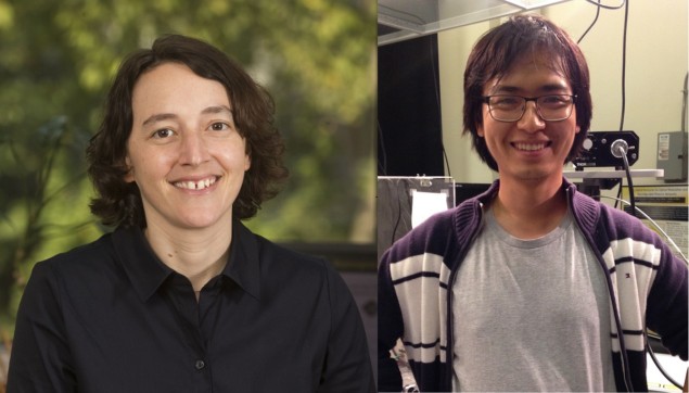
The team predicts that “Such an unprecedented strong light-matter interaction platform can facilitate the advancement of science in a broad range of applications, including low-power opto-electronics, nonlinear optics, and quantum optics.” The researchers Sharon Weiss and Shuren Hu
 The researchers Sharon Weiss and Shuren Hu
It all started with the theory
Shuren Hu, first author of the paper, now working as a Principal Engineer in Silicon Photonics at GlobalFoundries, told me a little bit about the journey and the people behind this work:
“Thinking back on this research project, it has been a really long journey, especially the experimental part. When Prof. Weiss and I first submitted the theory paper, we got very mixed feedback. Some reviewers were very interested, some doubted the feasibility of such a design. Thanks to our collaborators, we were able to fabricate such a photonic crystal with <10nm bowtie tip definition, and then to successfully characterize it. I want to give a shout out to our awesome collaborators and co-authors: Marwan Khater and Will Green are at IBM Silicon Photonics Group, and Ernst Kratschmer and Sebastian Engelmann are at IBM Material Research Lab. They together came up with several innovations in fabricating the bowtie photonic-crystal structures with high uniformity and v-groove depth modulation. Rafael Salas-Montiel at University de Technologie de Troyes also did a fantastic job characterizing optical mode distribution inside the structure using near-field scanning optical microscopy (NSOM).”
He also says that, together with Weiss, they are continuing to collaborate on this project through a new National Science Foundation grant, and they welcome new collaborations to further advance the science and applications of their bowtie photonic crystal.
14/9/2018 FROM PHYSICSWORLD.COM
Δεν υπάρχουν σχόλια:
Δημοσίευση σχολίου