Large tunnel magnetoresistance appears at room temperature in a miniaturized magnetic tunnel junction
22 Dec 2022 Isabelle Dumé
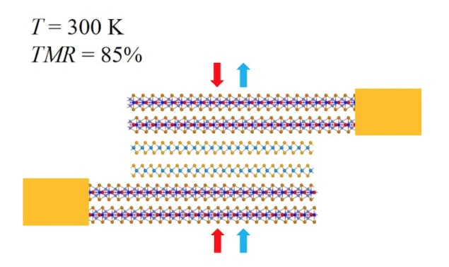
A large room-temperature TMR of 85% was obtained in all-vdW Fe3GaTe2/WSe2/Fe3GaTe2 MTJs. (Courtesy: K Wang)
Magnetic tunnel junctions (MTJs), which consist of two ferromagnets separated by a non-magnetic barrier material, are found in a host of technologies, including magnetic random-access memories in computer hard disk drives as well as magnetic sensors, logic devices and electrodes in spintronic devices. They do have a major drawback, though, which is that they do not operate well when miniaturized to below 20 nm. Researchers in China have now pushed this limit by developing a van der Waals MTJ based on a semiconducting tungsten diselenide (WSe2) spacer layer less than 10 nm thick, sandwiched between two ferromagnetic iron gallium telluride (Fe3GaTe2) electrodes. The new device also has a large tunnel magnetoresistance (TMR) at 300 K, making it suitable for memory applications.
“Such a large TMR in ultrathin MTJs at room temperature has never been reported before in all-two-dimensional van der Waals (vdW) MTJs,” says Kaiyou Wang, who directs the State Key Laboratory for Superlattices and Microstructures in the Institute of Semiconductors, Chinese Academy of Sciences, Beijing and is also affiliated with the Center of Materials Science and Optoelectronics Engineering at the University of Chinese Academy of Sciences. “Our work opens a realistic and promising route for next-generation non-volatile spintronic memories beyond the current state of the art.”
Room temperature ferromagnetism
Wang, who led the new device’s development together with Haixin Chang of the State Key Laboratory of Material Processing and Die & Mold Technology at Huazhong University of Science and Technology and the Wuhan National High Magnetic Field Center, attributes its large TMR to two features. The first is the intrinsic properties of Fe3GaTe2, which is ferromagnetic above room temperatures. “We have investigated the magnetoresistance of a number of van der Waals ferromagnet/semiconductor junctions for quite a few years in which the Curie temperature (the temperature above which a permanent magnet loses its magnetism) of the ferromagnet is far below room temperature,” he notes. “We found large magnetoresistance and efficient spin injection can only be achieved in nonlinear transport behaviour of ferromagnet/semiconductor junctions.”
In contrast to the materials Wang and colleagues investigated previously, Fe3GaTe2 (which the team discovered relatively recently) has a Curie temperature of more than 380 K. Its magnetic anisotropy is also comparable to (or even better than) that of CoFeB, a ferrimagnet widely employed in spintronics. (Unlike ferromagnets, where neighbouring magnetic moments are parallel to each other, in ferrimagnets the moments are anti-parallel but unequal in magnitude, yielding a residual spontaneous magnetism.) Importantly, Fe3GaTe2 and CoFeB both have highly polarized Fermi surfaces (the boundary between occupied and unoccupied electron energy states that defines many of properties of metals and semiconductors), which for CoFeB has meant that large spin-polarized electron sources operating at room temperature can be made from it.
A better spacer and device design
The second factor in the new device’s success, Wang says, is the high quality of the WSe2 barrier. “We discovered that using Fe3GaTe2 on its own is not enough and that we could only achieve a small room-temperature magnetoresistance (of around 0.3%) in one type of all-vdW spin-valves using a MoS2 spacer,” he explains. “We realized we needed a much better spacer and device design that allowed for highly efficient electron tunnelling.”READ MORE

Wang says the team’s work confirms that very large TMRs can be achieved at room temperature in all-vdW heterostructures, which he describes as a crucial step towards 2D spintronics applications. “Beyond that, the highly efficient spin injection into semiconductors could allow us to investigate semiconductor spin physics and develop new concept semiconductor spintronic devices,” he says.
Spurred on by their results, the researchers are now busy adjusting the thickness of the spacer layer in an attempt to further increase the TMR. One promising avenue they are exploring is to use the wide-bandgap semiconductor gallium arsenide (GaSe) or the insulator hexagonal boron nitride (hBN) as a spacer material.
They detail their present study in Chinese Physics Letters.

Isabelle Dumé is a contributing editor to Physics World
from physicsworld.com 29/12/2022

Δεν υπάρχουν σχόλια:
Δημοσίευση σχολίου