A smart approach to smart packaging
05 Apr 2018
This article first appeared in the 2018 Physics World Focus on Nanotechnology under the headline "Novelty when necessary"
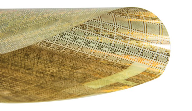
Flexible, low-cost integrated circuits could transform the market for “smart” devices and packaging, but as Catherine Ramsdale explains, building them requires more than just doing cool science Everyday electronics: Cheaper flexible integrated circuits open up new markets. (Courtesy: PragmatIC)
 Everyday electronics: Cheaper flexible integrated circuits open up new markets. (Courtesy: PragmatIC)
For more than 50 years, progress in the electronics industry has been guided by Moore’s law: the idea that the number of transistors in a silicon-based integrated circuit (IC) will double approximately every 18 months. The consequences of this doubling include a continual reduction in the size of silicon ICs, as it becomes possible to provide increasingly complex and high-performance functionality in smaller and smaller areas of silicon, and at progressively lower cost relative to the circuits’ processing power.
Moore’s law is an empirical rule of thumb rather than a robust physical principle, and much has been written about how, why and when it will eventually fail. But even before we reach that point, manufacturers are already finding that, in practice, the cost savings associated with reducing the size, or “footprint”, of ICs will only carry them so far. The reason is that below a certain minimum size, ICs become difficult to handle easily or effectively. For highly complex circuitry, such as that found in computers with many millions of transistors in a single IC, this limit on handling size may not be a consideration. However, for applications that require less complex circuits, the size constraint imposed by the physical aspect of handling ICs becomes a limiting factor in their cost.
This limit matters because as electronics extend further into daily life, there is a growing demand to introduce simple connectivity into everyday items – for example, in tracking and stock control for consumer goods such as milk, shampoo or deodorant that are produced in high volumes with lean supply chains; for interactivity in toys and games; and in “smart” packaging for pharmaceuticals to combat counterfeiting or sense whether medicines have been kept in the optimum temperature range. If we want to maximize the opportunities associated with the so-called “Internet of Things” and extend the range of smart devices beyond high-end consumer goods, then the price point for ICs needs to fall well below that of traditional silicon circuits.
A further factor driving the move away from silicon for low-cost electronics is that regardless of how small silicon ICs get, they are still rigid pieces of material. This makes it difficult to integrate them seamlessly into flexible or curved objects – such as shampoo bottles or juice cartons – without leaving a noticeable bump or impairing the object’s flexibility. Various techniques have been developed to try to correct this, such as covering or encapsulating the IC, but each of these creates challenges of its own as well as additional costs. Keeping track: “Smart” packaging requires low-cost connectivity. (Courtesy: PragmatIC)
 Keeping track: “Smart” packaging requires low-cost connectivity. (Courtesy: PragmatIC)
Getting flexible
The approach we have taken at PragmatIC is to use thin, flexible substrates, rather than rigid silicon, as the base for building our circuits. The low cost of the materials involved and the relatively low complexity of our target applications alters the economics around circuit footprint and overall IC cost. Accepting a larger footprint can lower capital expenditure because it means that ultrahigh-end precision tooling is not required to fabricate our circuits during the manufacturing process. In turn, for low-complexity applications, this can lead to a lower final IC cost.
The resulting flexible integrated circuits, or FlexICs, are thinner than a human hair, so they can easily be embedded in everyday objects. They also cost around 10 times less than silicon ICs, making it economically viable for them to appear in trillions of smart objects that engage with consumers and their environments. Since the technology was developed, PragmatIC FlexICs have been trialled in a wide variety of markets, including consumer goods, games, retail, and the pharmaceutical and security sectors.
In addition to the circuits themselves, PragmatIC has also developed a compact, automated system to manufacture FlexICs at high volumes. Whereas a conventional silicon IC fabrication facility, or “fab”, would typically require billions of dollars in upfront capital investment (not to mention considerable time) to set up, PragmatIC’s FlexLogIC™ “fab-in-a-box” model costs several orders of magnitude less and offers a greatly shortened build time. This system is also significantly smaller than a conventional silicon fab, and its self-contained nature makes it possible to install it in a wide range of manufacturing environments, such as label and packaging facilities.
We believe that this system has the potential to transform the market for flexible electronic solutions, as it enables non-electronics companies to become part of the supply chain. Because the FlexLogIC system is fully automated, it can be operated by companies with comparatively low levels of electronics expertise. The upfront design costs are also considerably lower, so new flexible electronic solutions can be developed, tested and rolled out in weeks (or eventually even in days) rather than months, and with reduced risk. This reduction in both cost and time enables a scalable distributed production model. Compared with silicon ICs, where a few huge foundry companies produce most of the world’s supply, the FlexLogIC model can support a large number of global manufacturers, across multiple locations.
The resulting flexible integrated circuits, or FlexICs, are thinner than a human hair, so they can easily be embedded in everyday objects; and they cost around 10 times less than silicon ICs
Model differences
Whenever you try to bring new technologies and products to the mass market there are always challenges, and the products discussed above are no exception. In our experience, one of the ways to overcome these hurdles – perhaps a bit counterintuitively for a hi-tech industry that thrives on innovation – is to avoid adding novelty unless it is absolutely necessary.
As an example, we have found that using off-the-shelf equipment and components wherever possible is a must. Anything bespoke immediately introduces challenges. There will be additional upfront costs. The level of maintenance support from the manufacturer will not be the same as with standard tools, and it will be more difficult to find and hire knowledgeable production staff who have used similar tools before.
The mantra of “novelty only where needed” also stretches back to the design phase, where the underlying physics of our devices has a direct impact on the assumptions we use to simulate their behaviour. PragmatIC uses devices built on metal oxide semiconductors, where charge carriers move via band conduction in spherically symmetric s-orbitals with a high degree of spatial overlap. This differs significantly from conduction in silicon, where there is strong spatial directivity in the sp3 orbitals that control the conduction pathways. One implication of this difference is that, whereas any disruption of silicon’s ordered lattice will significantly impair the mobility of charge carriers, the high degree of orbital overlap in metal oxides means that carrier mobility is not sensitive to the film structure in the same way.
Once we had got to grips with the limitations of our models, we had to do some additional work to avoid building inconsistencies between the model device and the real one into our simulations. Some of this work was theory-based, but there was also a lot of experimentation: PragmatIC builds from the ground up and evaluates devices in different scenarios to understand how performance compares with the predictions from the models. This informs slightly more complex circuitry, which is then evaluated in the same way and so on in an iterative process. In 20 or 30 years, theoretical models based on metal-oxide semiconductors may have evolved to the point where we can avoid this kind of trial-and-error work, but right now, the highly developed models that exist for silicon are simply not available for our system.This presented us with a conundrum. We had selected commercial circuit design tools because they are well supported, regularly updated and familiar for external users. However, commercially available design tools predominantly use well established silicon-based models to predict and describe how IC devices will behave, and unfortunately, we found that these models did not fully describe the physics of our devices. For example, in crystalline silicon transistors, an increase in temperature will reduce the mobility of charge carriers in the transistor, but in amorphous oxide transistors the mobility will actually increase with temperature. Consequently, we had to work out how our devices’ behaviours differed before we could understand where the models were likely to be accurate, and where they were not.
The right approach
There are usually one or two key differentiators that make a product unique and could create opportunities in the market. However, the typical consumer will not be interested in how this unique product is made, only in its final functionality. Although it is always more stimulating on a personal or intellectual level to be trying something new and figuring out how to get it to work, if your exciting new technique will increase costs without augmenting the functionality, then it is a commercial non-starter. Hence, unless a new approach actually provides a commercial advantage, it should not be pursued, no matter how innovative it is.
By the same token, we know that flexible electronics will not replace silicon electronics in areas where silicon excels. In terms of actual computing, there is nothing our technology can do that silicon cannot. However, in areas where silicon falls down, a new approach overcomes the commercial disadvantages of doing things differently – and thus offers a route to new implementations of electronics in everyday household items that have not, until now, been economically viable.
Enjoy the rest of the 2018 Physics World Focus on Nanotechnology in our digital magazine or via the Physics World app for any iOS or Android smartphone or tablet.
Catherine Ramsdale is vice-president of device development at PragmaticIC
6/9/2018 FROM PHYSICSWORLD.COM
Δεν υπάρχουν σχόλια:
Δημοσίευση σχολίου